

Silakan tinggalkan kami pesan
Privacy statement: Your privacy is very important to Us. Our company promises not to disclose your personal information to any external company with out your explicit permission.
Select Language

introduction
With the development of deep sub-micron processes, the capacity and density of FPGAs continue to increase. With its powerful parallel multiply-accumulate (MAC) capability and flexible dynamic reconfigurability, FPGAs are widely used in many fields such as communication and imaging. However, in the implementation of complex algorithms, FPGAs are not as convenient as embedded processors. Therefore, when designing systems with complex algorithms and control logic, they often need to be combined with embedded processors. This is SOPC (System on a Programmable chip, Programming system-on-a-chip) technology. SoPC is the product of a combination of SoC and FPGA, with a single programmable reconfigurable chip to perform the main functions of the entire system. The SoPC design is flexible and can be designed in schematic, hardware description language or even C/C++ high-level language. It also has the features of reconfigurability, reduction, and expandability. It is easy to upgrade. SoPC combines the advantages of both SoC and FPGA with the following features:
● Rich IP core resources, including general IP cores and dedicated IP cores
● Programmable, easy to design, compile, download and debug in the system
● Built-in embedded soft core processor, memory, peripheral interface controller
● A large number of programmable refactoring logic resources
●Powerful clock management circuit
● Support multiple I/O interface standards
In addition, due to the reduced transmission line distance between the processor and the memory, SoPC has obvious advantages over board-level systems in terms of speed, signal integrity, and electromagnetic compatibility.
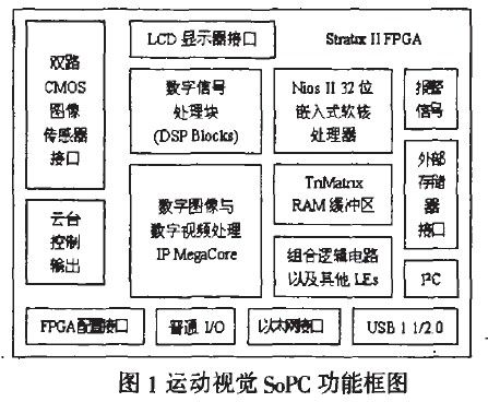
1 functional block diagram
Based on the development of digital video visual acquisition and processing board level system, this paper uses SoPC to realize the design of motion vision processing and control system. The hardware uses Altera's Stratix II series of FPGAs, and software development tools include Quartus II, Nios II 5.1 IDE, DSP Builder, MegaCore IP Library 5.1 and Matlab 7.0. The working principle of the whole SoPC system is: the video image data collected by the camera is input by the image sensor interface; the digital signal processing block and the digital image and the digital video processing IP core complete the processing of the video image, such as motion detection, segmentation, feature extraction, compression, etc.; The Nios II embedded processor mainly completes the control functions of the entire system; the I2C bus is used to access the internal registers of the CMOS image sensor; the PC can access the SoPC through the USB interface, and if the distance is long, the data can be transmitted through the Ethernet port. The video image and its processed result can be stored in the CF card, FLASH and other storage media through the external memory interface, or directly displayed on the LCD screen through the LCD display interface. The functional block diagram of the motion vision SoPC is shown in Figure 1:
2 video capture module
This module is mainly responsible for video image acquisition, camera parameter setting and pan/tilt stepper motor control. Among them, the camera internal control register can be set through the I2C bus. In FPGAs, there are two ways to implement I2C bus controllers: one is implemented in software simulation in Nios II; the other is using third-party IP cores such as Scivox, CAST, and Digital Core Design. These IP cores have operating parameters that can be set as needed. Take the I2C bus controller provided by CAST as an example, the transmission rate is up to 100Kbps, and it can work in four modes: main transmitter mode, main receiver mode, slave transmitter mode and slave receiver mode. The dual CMOS image sensor interface controls the timing of video image acquisition, frame synchronization and line synchronization; the pan/tilt control signal controls the rotation of the two stepping motors of the gimbal according to the result of the video image processing. These two modules need to be developed by themselves to form an IP core with independent intellectual property rights.
3 video image processing module
The module includes NiosII 32-bit embedded processor, digital signal processing block, digital image and digital video processing IP MegaCore, and other logic circuits, which are the focus and core of motion vision processing and control SoPC design, respectively Partial introduction.
(1) Nios II embedded processor
The Nios II embedded processor is a general-purpose RISC-based CPU that targets a wide range of embedded applications. In the Nios II IDE integrated development environment, add and set the relevant parameters according to the operation prompts, and generate a Nios II embedded processor in a few minutes. The hardware development process is:
1 Analyze the functions and performance of the system
2 Start SOPC Builder and select the specific FPGA model.
3 Define modules such as CPU, peripheral devices, storage systems, etc.
4 Assign a base address and interrupt request number (IRQ) to each module
5 Generate the Nios system module, pin lock, compile the software development process as:
1 Launch the Nios II IDE in SOPC Builder
2 Create a C/C++ software project and specify the target hardware
3 Use the engineering template to write the corresponding program
4 After compiling, you can download and run to the hardware.
The Nios II IDE can be written in C/C++ or assembly language with file extensions .c and .s respectively. A single Nios II/f CPU requires approximately 1800 LEs. If additional timers, peripherals, etc. are added, the occupied logic unit will increase further.
(2) Digital signal processing block
The Stratix II family of FPGAs has digital signal processing blocks (DSP Blocks, DSP blocks). The digital signal processing block can support multipliers (9×9, 18×18, 36×36) and operation modes (multiplication, complex multiplication, multiply-add and multiply accumulate) with different data widths, provided by each DSP block. 2.8 GMACS DSP data throughput. The largest Stratix II device EP2S180 contains 96 digital signal processing blocks internally, providing 284 GMACS throughput and supporting 384 18×18 multipliers. In addition, the digital signal processing block adds new rounding and saturation support for easy import of DSP firmware code into the FPGA. Some applications, such as voice processing, can use rounding and saturation because the storage buffer for storing data is fixed width. Now with a digital signal processing block that supports rounding and saturation, it is easy to import a DSP processor-based design into an FPGA for implementation.
DSP system design on Altera's programmable devices requires development tools that support both advanced algorithms and hardware description languages. MathWorks' MATLAB and Simulink system-level design tools provide algorithm development, simulation, and verification capabilities. Altera's DSP Builder combines these tools with Altera's development tools to provide a DSP development platform for system design, algorithm design, and hardware design sharing.
(3) Video image processing
The IP core third party provides a number of customizable IP cores for communication, image encoding and decoding, and video processing. Proper use of these IP cores can greatly reduce development time while ensuring performance and reliability. The color space conversion IP is described below.
CSC (Color Space Convertorr) is an IP core dedicated to image color space conversion in the MegaCore IP library file provided by Altera Corporation. Compared with software conversion, it has obvious speed advantage and flexibility:
● Complete one pixel conversion per clock cycle
● In Stratix series FPGAs, the clock frequency is greater than 200MHz
● Supports interchange between RGB and YCbCr, YUV
● Users can customize the correlation coefficient of the transformation matrix
● Support for signed and unsigned numbers
4 RAM data buffer
Input and output data width is 2 ~ 32b 4 RAM data buffer Stratix II series FPGAs contain up to 9Mb of on-chip RAM. These RAMs use the TriMatrix memory architecture and include three sizes of embedded memory blocks: 512b M512 block, 4Kb M4K block and 512Kb M-RAM block, each of which can be configured to support various features such as single port. RAM, dual port RAM, FIFO, etc., provide solutions for large storage applications.
5 external memory and peripheral interface
The Stratix II family of FPGAs is optimized for reliable data transfer from external memories and supports the latest memory interfaces for accessing off-chip memory. Using Stratix II's advanced device features and customizable IP cores, developers can quickly and easily integrate a wide range of high-capacity memory devices into complex system designs. Stratix II supports a variety of the latest storage interfaces. The Stratix II family of FPGAs is connected to the peripherals via an Avalon switched bus. The Avalon Switched Bus is a proprietary internal interconnect technology developed by Altera that uses minimal logic resources to support data bus multiplexing, address decoding, wait cycle generation, peripheral address alignment, interrupt priority assignment, etc. . Peripheral Interfaces Customizable IP cores include USB, I2C, Ethernet, PCI, etc. These IP cores are mostly provided by third parties and can be used for free trials or for partial purchases. The USB2.0 controller and Ethernet interface controller used in this system are provided by Mentor.
6 clock management circuit
Stratix II family of FPGAs with up to 48 high-performance, low-offset global clocks for high-performance functions or global control signals; up to 12 programmable phase-locked loops (PLLs) with complete clock management and frequency Synthesis capabilities, including clock switching, PLL reconfiguration, spread spectrum clocking, frequency synthesis, programmable phase shifting, programmable delay skew, external feedback, and programmable bandwidth. Stratix II has two general-purpose PLLs: Enhanced PLL and Fast PLL. Enhanced PLLs feature rich external support, spread-spectrum clocking, programmable bandwidth, etc. The fast PLL is optimized for high-speed differential I/O interfaces with Dynamic Phase Adjustment (DPA). These high-speed clock networks combined with a rich PLL provide a powerful guarantee for the system to operate with minimal clock skew.
7 Other components of SOPC
The FPGA configuration interface is used for SOPC configuration, compilation and online debugging; the LCD display interface can be connected to the LCD screen; the alarm signal is the sound or photoelectric signal emitted when detecting and identifying the moving target, which can be used for security; standard I/O The port is reserved for future upgrades.
Innovation: Before the concept of SoPC was put forward, the integrated design of electronic systems was mainly based on board level. This design method is more and more difficult to achieve with the increasing clock frequency of the system and the increasingly complex circuit functions, electromagnetic interference and Signal integrity issues are becoming more prominent. By optimizing the layout and routing of the PCB, it is no longer sufficient to meet the transmission and processing requirements of high-speed signals. With the continuous development of the semiconductor industry, the programmable system-on-chip will become the mainstream of future electronic product development and design with its high performance, reliability, low power consumption, cost and good portability. The motion vision SoPC better solves a series of problems in the board-level circuit, and can be widely used in many fields such as security monitoring, visual navigation, intelligent transportation, etc., and there will be a good market prospect.
Pengarang:
Mr. Simon Feng
Phone/WhatsApp:

July 14, 2023

July 06, 2023
Email ke pemasok ini
Pengarang:
Mr. Simon Feng
Phone/WhatsApp:
July 14, 2023
July 06, 2023

July 14, 2023

July 14, 2023
Tel: 86-13063807111
Whatsapp: +8613063807111
Alamat: 3rd floor, building 3, no.1988, Zhuanshi road, XiangCheng district, Suzhou city,China, Suzhou, Jiangsu China
Situs web: https://id.yuzenvision.com
Privacy statement: Your privacy is very important to Us. Our company promises not to disclose your personal information to any external company with out your explicit permission.
Fill in more information so that we can get in touch with you faster
Privacy statement: Your privacy is very important to Us. Our company promises not to disclose your personal information to any external company with out your explicit permission.